
由2D基于2D材料的神经形态设备启用的高级AI计算
作者:Bae, Sang‑Hoon
介绍
依靠Neumann架构特征的经典计算顺序处理,其中内存和逻辑单元的分离是通过总线结构互连的1,,,,2,,,,3。这种架构,加上摩尔定律预测的电子设备的微型化,在过去几十年中实现了计算能力的指数增长4,,,,5。但是,由于记忆和处理单元之间的数据传输负载的增加,冯·诺伊曼瓶颈随着时间的推移而表现出来,这在此过程中最多可以消耗高达60%的计算能量,并限制了设备集成密度,从而极大地阻碍了性能。6,,,,7,,,,8,,,,9。此外,数据的爆炸性增长加剧了数据量和总线容量之间的不平衡。因此,一种现象出现为记忆墙,它限制了现代计算系统的速度和效率,尤其是在人工智能(AI),机器学习和大数据分析等数据密集型应用程序中10,,,,11。
受人脑的启发,神经形态计算引起了极大的关注,因为它的出色潜力可以模仿大脑的出色能量效率和计算能力。与依赖二进制逻辑的传统数字系统不同,神经形态系统通过神经元和突触的动态相互作用来利用模拟和事件驱动的处理,从而提供了功率效率和处理非结构化数据的优势。为此,二维(2D)材料提供了几种独特的特征,使他们能够克服神经形态计算中传统的二维(3D)散装材料所遇到的局限性12,,,,13,,,,14。由于它们的原子厚度,2D材料具有出色的电气性能,例如高载体迁移率和低功耗,这对于降低神经形态设备的功耗至关重要。此外,2D材料由于其出色的电子特性而用作有希望的构建块,而高厚度的高机械柔韧性使范德华(Van der Waals)(VDW)堆叠不同的材料以形成VDW异质结合,在引入新功能的同时,可以保留单个材料的性能13,,,,15,,,,16。这种原子较薄的厚度还促进了整体式3D整合(M3D),具有高垂直整合密度的潜力,从而能够开发密集包装的,可伸缩的神经态电路,可以模仿生物神经网络的复杂连通性17。此外,2D材料的出色可调节性还可以更精确地控制突触重量,这对于人工神经网络(ANN)中短期可塑性(STP)和长期可塑性(STP)和长期可塑性(LTP)至关重要的突触重量至关重要。18,,,,19。这些特性共同使2D材料能够应对阻碍常规神经形态系统的可扩展性,功率效率,模拟计算和突触可塑性的挑战。
在这里,我们使用2D到3D存储器设备及其高级配置的2D材料进行了分类和实现的设备体系结构。还讨论了集成2D材料对神经形态回路的系统级含义,还使用了可以提高神经形态计算的性能和效率的先进方法进行了讨论。此外,我们回顾了与各个行业相关的神经形态系统的潜在应用。在结论部分中,还概述了高级2D神经形态计算系统的实际挑战,新兴的机会和观点。
基于2D材料的突触设备
神经形态突触设备能够在停用后能够保留其电状态,并且由2D材料组成的神经型突触设备已成为有希望的研究领域。这些设备通常可以分为两种类型:两端(2 t)存储器和三端(3 t)存储器设备,其中2D材料主要用作2 t设备中的介电或工作层,以及3 t设备中的介电设备或通道层。此外,已经开发了2 t和3 t突触设备和多末端设备的混合结构,以增强记忆设备的功能20,,,,21,,,,22。使用2D材料的回忆录通常以跨杆阵列结构排列23并分为四个配置:1 Memristor(1âm)24,1二极管1 Memristor(1d1m)25,1选择器1 Memristor(1S1M)26和1个晶体管1 Memristor(1T1M)17。每种配置都表现出独特的特征,可提高当前方向性和整体回忆性功能。
2 t突触回忆录具有简单的结构,主要由两个导电电极和两者之间的活性层材料组成。基于主动层的2D材料可以构建具有低能消耗和空间的大型横梁阵列。回忆录的基本概念是基于在两个不同状态之间切换设备的基础:高电阻或低极化状态(HR)和低电阻或高极化状态(LRS)27。在电阻内存中,从HRS转移到靠近导体的LR的过程被称为设置操作,而反向过程称为重置操作。这些状态可以表示为0和1的二元值,在该二进制值中,低阻力状态(在状态下)和高阻力状态(OFF状态)。利用这种机制,可以模拟各种突触功能,包括兴奋性突触后电流(EPSC),峰值依赖性可塑性(STDP),配对脉冲促进(PPF)和峰值速率依赖性可塑性(SRDP)28。
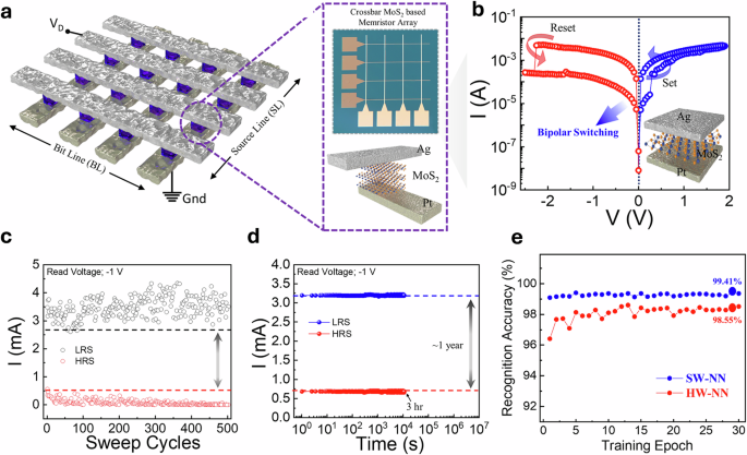
电阻开关内存(RSM)(2ât)设备是具有快速开关速度和可扩展性的有希望的突触设备。RSM的电极材料通常由活性金属材料(例如Ag和Cu)组成,该材料参与导电丝的形成,或者用作稳定的反电极的惰性金属材料(如AU和PT)29,,,,30。此外,各种过渡金属二甲元化(TMD)半导体材料,包括H-BN,MOS2,WS2,WSE2和摩西2,已被证明是活跃的层材料,即使在重复的压力下,也可以增强开关性能并减轻设备降解31。基于导电丝的形成:电化学金属化(ECM)和价变化机制(VCM)有两个主要的电阻切换机制。ECM设备由位于由活性金属制成的上电极和由惰性金属制成的下部电极之间的介电层组成,用于离子迁移,以形成和溶解金属丝32,,,,33。VCM设备具有由惰性金属制成的电极,介电层是TMD34,,,,35。当将电压施加到电极上时,会产生电场,从而诱导可逆的氧化和还原反应,从而导致导电丝的形成。例如,基于MOS提出了一种新型的多级电子突触设备2Memristor阵列(图。1a,,,,b)36。该设备利用具有高度结晶的MOS的4â€4横杆结构2电影。薄的mos2层(〜2.1 nm)可实现低压切换,并以超过500个扫描周期的耐力表现出出色的记忆性能,保留时间约为104S(图。1C,,,,d)。提出的MOS2Memristor Array在深神经网络(DNN)中达到了高识别精度,精度为98.55%(图。1e)。

拟议的4âââ€4横杆回忆录阵列的建筑示意图,基于大区域直接成年MOS2带有单个Memristor的3D部分视图36。bMOS的双极记忆开关曲线22.5 v和2 v之间电压下的Memristor设备。c拟议的Memristor设备的内存操作在耐力的方面最多可扫至500个扫描循环,在1 -V的读取电压下d保留,测量高达104在1 v的读取电压上。e每个训练时期的SW-NN和HW-NN的识别精度图。相变存储器(PCM)(2ât)是一种非易失性存储器(NVM)技术,利用材料的可逆相变特性来存储数据,通过应用电脉冲来存储数据。
与散装PCM相比,由于其原子水平的厚度,2D材料对外部刺激更为敏感。结果,2D材料中的相变很容易被各种外部刺激(例如应变,离子插入或静电掺杂)诱导37。与传统的相变材料不同,在非晶状态和结晶状态之间切换不同,具有各种多晶型物的TMD表现出结构相变。特别是mos2在六边形结构(2H相)和扭曲的八面体结构(1ât或1ât或1th²相)之间进行相变21,,,,35。此外,提出了2D钾间隔锰二氧化碳中电场引起的可逆相变(K-Mnoâ)37。这些晶体的薄度高达5 nm,原子层厚度为0.7 nm,钾离子自发插入MNO2合成过程中的结构,有助于离子传导(图。2a,,,,b)。在大约10 v的中等偏置条件下,观察到不同的相变,其中材料在分层和尖晶石结构之间切换(图。2C e)。发现设备的电压衰减时间常数(»)为81±10 s/歧程,并且设备在5,600多个增强和抑郁的周期中保持了其性能。

MNO分层和隧道多晶型的代表性示意图2而且,MN3o4。b2D K-MNO的光学显微镜图像2蓝宝石基材上的晶体37。c我是从石墨/k-mno的v周期2/石墨回忆设备。d示意图描述了当应用无偏见的面板I并应用偏置时面板II时的条件。典型的3 t晶体管设备由包括电极,介电层和通道层的结构组成。
栅极电极用作突触前节点,而源和排水电极充当突触后节点。与2 temristors不同,3 t晶体管具有一个栅极终端,该端子允许通过动态电阻开关调节通道电导,从而实现了多级数据存储。可以通过多门调制来实现出色的突触重量更新,从而使该设备适合在神经形态计算系统中学习。此外,基于晶体管的结构能够最大程度地减少潜行,减少功耗,支持模拟计算并实现大规模并行处理38。
首先,在浮栅内存或基于电荷捕获的内存结构中模仿突触的设备通常由用于存储器的三明治结构组成39。电荷陷阱层插入门和通道区域之间以存储电荷40。该设备的优势在于其技术成熟度,从过渡晶体管继承,并且隧道层的存在可确保长期保留无电荷损失。该机制通过在控制门上施加电压,从而创建电场,使电子隧道进入电荷诱捕层41。一旦电子隧道,它们就会被困在该层中,该层通常由陷阱或可以长时间存储电子的缺陷设计。2D材料的杂缝充当载体陷阱,作为杂结和材料共存缺陷的能量带比对,以调节通道的电导率。基于2D半导体材料提出了超快的双极闪存,从而实现自动化内存计算42。关键结构由Al'Oâ,Hfoâ,H-Bn和Wseâ的层组成,分别用作阻断氧化物,电荷捕获层,隧道屏障和半导体通道(图。3a)。当施加栅极电压时,电子隧道进入HFO2层并存储在那里,将通道变成N型。一旦收费被困在HFO中2层,它们调节WSE的费米级2通道,确定该通道是表现为N型还是P型(图。3b)。双极闪存的编程速度约为20 〜30 ns,比常规闪存的速度快三倍(图。3C)。此外,它还显示出超过800万个周期的耐力,每个Mac操作仅消耗5 fj的能量,展示了极低的功耗(图。3D)。

双极闪光阵列的插图,包含4台设备42。b存储不同电荷的设备的带图。左:负脉冲后,将孔存储在捕获层中。右:在正脉冲后将电子存储在捕获层中。c电子和孔电流双扫向传输特性(我DS相对vg)N型(编程为19 v/50 ms)。d设备耐力测试。e具有自激活CNN模型的测试精度。电解质层的突触设备使用电解质作为栅极绝缘体。
它们可以大致分为两种类型:静电调制和电化学掺杂。在静电调制的情况下,半导体层由电解质层离子不渗透的材料组成。当施加栅极电压时,离子的移动受到影响,所得的电场会导致离子在半导体和电解质层之间的接口处积聚,形成电动双层(EDL),以调节设备的电导率状态43,,,,44。相比之下,电化学方法也形成了电动双层,但是电解质层的离子可以渗透到半导体层中,从而进一步调节通道电导45,,,,46。电解质层的突触设备在电导状态的线性和对称更新中具有优势。但是,由于它们的操作依赖于离子的物理运动,因此它们的电导状态更新较慢,并且更容易受到热效应。
铁电场效应晶体管(FE-FET)是通过将铁电特性整合到常规薄膜晶体管(TFT)结构中而开发的47。铁电材料表现出用于记忆功能的自发极化。它们的高介电特性有助于增加层厚度,以防止电流泄漏,并且应仔细设计极化层以适应各种2D/3D结构48。这些材料中极化的方向可以通过外部电场来控制,从而影响其电导率49。2D铁电材料可以用作通道材料,从而提供了设备性能的潜在改进。Yeonsu Jeong等。报道了基于Mose/Mos杂孔的FET的开发和应用,用于多级记忆,多尺度显示和突触功能50。Mose/MOSâ杂结式FET是使用底部栅极金属 - feRroelectric-Metal-Metal-unsulator-semicDuctor(MFMIS)结构构建的(图。4a,,,,c)。该设备由Mose/Mosâ杂结组成,作为通道层,HFO铁电层和金属栅极电极组成。该结构旨在利用HFO层的强电荷捕获能力和极化特性,从而可以精确控制通道电导(图。4d,,,,e)。Mose-/MosâFets具有出色的电气性能,例如高/OFF电流比超过10â·excles,在10英寸循环上的耐用耐力以及最小的设备对设备变化约为0.5%(图。4b)。桌子1提供了神经形态计算的突触设备的摘要,以进行全面的理解。

神经元系统中生物突触的示意图和神经形态功能的突触堆栈通道FET。b摩西的转移曲线2/mos2堆栈通道记忆FET,显示不对称记忆滞后行为,如V的双扫GS。cOM摩西的图像2/mos2堆栈通道内存FET。d摩西的2D示意性结构2/mos2堆栈通道FET描述摩西的电子陷阱2/mos2异径接口e。摩西带图2/mos2在相应d84。表1基于2D材料的2 t和3 t内存设备的摘要神经形态系统演示由于已广泛研究并被证明是突触设备有希望的,因此对神经形态系统的研究也加速了。生物神经网络涉及两个主要阶段:学习和推论。神经形态系统旨在模仿这些阶段。为了在神经形态系统中实现这些功能,必须设计能够准确存储权重和处理输入/输出操作的系统。神经形态系统的实施需要三个关键组成部分:突触,神经元和外围电路。
突触
负责信息存储和处理。
-
他们通过调节神经元之间传播的信号强度(即突触权重)来模仿生物突触的学习和记忆功能。
这可以使用各种新兴内存技术(例如回忆录或备忘录)来实现,它们会根据先前的信号动态调整其电气性能,从而使系统能够学习和适应。2。
-
神经元
从突触中接收输入,集成这些信号并根据输入生成输出。例如,在模仿尖峰神经网络(SNN)的系统中,神经元一旦超过阈值,神经元会积累输入信号并产生尖峰,从而模拟了生物神经元的行为(例如,泄漏的集成和传火(LIF)模型)。然后将这些处理的信号传输到其他神经元或突触,从而促进整个网络的通信。
-
3。
外围电路管理神经元与突触之间的相互作用,促进学习和推理,并确保实现的神经形态系统的平稳运行。对于输入,有必要放大从传感器或人为创建的输入获得的电信号,以提供足够的电压,以适用于制造的神经元和突触所需的电压。还需要其他电路(例如反馈电路和激活功能)来实施捏造的神经元和突触的操作。
对于包括SNN和DNN在内的ANN的硬件实现,将突触,神经元和外围电路集成到大型阵列尺度上的互连系统至关重要。当这些组件无缝集成时,系统会紧密模拟生物神经网络,复制核心功能,例如学习,记忆和认知。这种完整的整合对于实现在人脑中观察到的适应性和有效的处理至关重要的,例如模式识别,决策和感觉处理。Yooyeon Jo等。通过集成突触和神经元报告了SNN系统的配置51。数字5a说明了使用RRAM和被动组件在面包板上构建的小型SNN系统的示意图,以模仿人类的神经网络。在该系统中,挥发性RRAM充当发送和接收信号的神经元,而非挥发性RRAM充当决定信号强度和传播的突触。输入信号电荷电容器c1在RC电路中,当超过特定的阈值时,挥发性RRAM会打开,通过突触将信号传输到后神经元。像神经前一样,后神经元在RC电路超过特定阈值时激活并生成输出信号。为了现实地模仿人类神经传播中的LIF行为,电阻与电容器并联连接。另外,将二极管和放大器放置在突触和神经元之间,以防止逆转泄漏并确保对后神经元后的足够信号传递。通过观察每个节点处的电压以响应相同的输入脉冲,我们表明,神经元后的输出尖峰频率取决于图2中的突触电导。5b。此外,输出尖峰的数量不仅受突触电导的影响,而且还受RC延迟的影响(Rs× Cmem)和输入电压脉冲条件在面包板上配置。因此,找到最佳参数对于神经形态系统应用至关重要。所提出的SNN系统使用实验获得的神经元和突触的数据在784â100â100的网络体系结构中进行了模拟。输入数据转换为泊松尖峰列车,并根据像素值调整每个神经元的发射速率。该模拟的准确度为83.45%,与90.65%的理想精度相当。确保足够的设备性能对于成功的神经形态系统实现至关重要。

电路图的示意图51。bANN的瞬态电测量,具有三种不同电导的突触设备。c横杆阵列中1T1M电池的横截面扫描透射电子显微镜图像52。d所考虑的SNN的结构。每个MNIST图像都被重塑为784â-1列矢量,并且像素的强度根据输入神经元的发射频率进行编码。唯一可以训练的突触是将输入层与兴奋层连接的突触,它们以基于CMOS H-BN的1T1M细胞的STDP特征进行建模。e拟议的神经元突触神经元块的电路示意图结合了基于H-BN的1T1M细胞和CMOS电路。颜色表示完整的神经元(灰色周围的盒子),核心块(浅蓝色盒子)和单个构件(浅红色盒子)。fMOS的示意图2 -xoxCVD生长石墨烯电极的结构54。g光学传感器的特征提取操作。h分类器仿真的单层感知器照片回忆录阵列的示意图。同一类(颜色)的光序列器并行相互连接,以生成激活函数的输出电流。Kaichen Zhu等。提出了与CMOS系统和2D RRAM集成的神经形态系统杂种
52。他们证明了通过图2中的CMOS后端(BEOL)过程转移H-BN纳米片的1T1M阵列的单个单元。5C。与被动的备忘录设备相比,所得的设备显示出改善的电气特性,使其适用于神经形态系统的实现53。基于这些属性,使用MNIST数据集上的SNN进行了无监督的学习模拟,达到90%的平均准确度。所提出的系统网络体系结构,如图2所示。5d,由784个输入神经元,400个兴奋性神经元,400个抑制性神经元和10个输出神经元组成。此外,图。5e说明了提议的CMOS电路用于电子神经元的硬件实现,该电路通过香料模拟进行了验证。拟议的系统使用了混合配置,将基于2D材料的RRAM技术与CMOS技术集成在1T1R结构中以进行突触,而CMOS电路则提议模仿生物神经元的LIF行为。电路中包括一个差分对以计算负重,而矢量 - 矩阵乘法(VMM)操作同时发生在神经形态阵列中。为了确定差分对输入,将输入选择电路放置在开始时,而末端的逆变器放大器确保当输出神经元的膜电位超过阈值时,确保了尖峰的产生。香料仿真结果证实,尖峰后产生的频率取决于峰值的时机,因为根据SNN中的STDP学习规则调整了权重。膜电势从相同的输入尖峰增加的量根据重量而改变。当特定节点的电压超过阈值时,逆变器放大器的操作通过产生尖峰来证明LIF的火行为。这项研究强调了将突触设备整合到大规模阵列中以进行神经形态系统实现的重要性。它还强调,成功的神经形态系统不仅需要改善突触的电气特征,而且还需要对神经元实施的同时研究。
输入注意事项对于实用的神经形态系统演示也至关重要。尽管大多数研究使用半导体分析仪(例如B1500)控制输入,但Edge Computing应用程序可以直接从传感器中获取输入。小福等人。报道了使用非挥发的光学磁盘阵列的集成传感器和神经形态系统54。数字5f显示了基于石墨烯/MOS的非挥发光媒体的结构2 -xox/石墨烯(石墨烯/M/石墨烯),用于模仿人类视觉系统。人类视觉系统扮演两个重要角色:首先,它通过提取来组织预处理的图像,其次,它对通过眼睛获得的数据进行了分类。CNN操作模拟了预处理任务,并且Opto-Memristor阵列用作固定的内核来提取输入的特征,如图2所示。5G。这种预处理通过从模拟图像中提取特征来降低后续操作的计算复杂性。数字5H还说明了使用神经网络实现的眼睛的分类功能。通过预先调整光学磁盘阵列的权重,它可以用作带有Mân输入和5个输出的单层感知器。因此,非易失性光学阵列阵列在减少输入和处理阶段之间的延迟中起着关键作用,模仿了人类的视觉系统。总之,尽管基于2D材料实施大规模神经形态系统的研究仍然有限,但对小规模系统的研究仍在稳步发展,为将来实施真正的神经形态计算铺平了道路。
神经形态计算的新兴应用
近年来,2D材料和神经形态计算都取得了重大进步。2D材料(例如石墨烯与神经形态体系结构)的组合带来了独特的优势,例如增强的电导率,可伸缩性以及通过SNN模仿大脑样功能的能力。这些系统有可能通过提供实时自适应学习,并行处理和大量能源效率来彻底改变各个领域。应用程序涵盖了各种领域,包括自主系统,机器人技术和医疗保健,神经形态系统可以在人类感觉能力和机器智能之间弥合差距。
自主驾驶中的神经形态系统:增强视觉
Neuromorphic vision systems are transforming autonomous technologies by addressing key challenges in real-time decision-making, adaptive navigation, and low-light imaging.Central to this transformation are photomemristors, which represent a significant advancement in neuromorphic vision by integrating sensing, memory, and computation into a single device.
In particular, VOâ‚‚-based photomemristors further extend the potential of neuromorphic systems by incorporating synaptic plasticity, a core feature of biological neural networks.Their unique phase transition properties allow for adaptive preprocessing, noise reduction, and enhanced object classification in UV-sensitive imaging scenarios.Li等。showed that these devices improved image classification accuracy from 24% to 93%, illustrating their transformative impact on autonomous navigation and environmental monitoring55。These photomemristor technologies enable neuromorphic systems to achieve high-resolution imaging and adaptive decision-making, particularly in variable lighting conditions such as urban nightscapes and rural highways.By integrating these advancements, photomemristors serve as critical components in intelligent autonomous vision systems.
Complementing photomemristors, spiking neurons constructed with 2D subthreshold transistors (2D-ST) have emerged as a pivotal innovation in neuromorphic vision, particularly for enhancing real-time obstacle detection in autonomous vehicles.These systems effectively process data from sensors and cameras, enabling vehicles to respond dynamically to changing road conditions, obstacles, and traffic.This capability is critical for ensuring both energy efficiency and safety in self-driving cars, where rapid decision-making is essential.Thakar et al.demonstrated that 2D-ST neurons mimic the behavior of biological neurons, such as the lobula giant movement detector (LGMD) found in locusts, which specialize in detecting looming objects (Fig.6a)56。The biomimetic design allows the system to register spikes efficiently as stimulus intensity increases, which mirrors the natural neural response to approaching objects (Fig.6b)。These spikes increase in frequency as objects approach, peaking just before potential collision, ensuring a fast response time crucial for navigation (Fig.6c)。Moreover, the 2D-ST system exhibits exceptional energy efficiency, consuming as little as 3.5 pJ per spike for obstacle detection in real-time scenarios, and less than 100 pJ per detection event overall.Such efficiency, combined with rapid response times, makes it an ideal solution for energy-constrained applications like autonomous vehicles.Additionally, as shown in Fig.6d, the system generates more spikes for inputs representing higher threat levels.For receding stimuli, it maintains efficient spike activity and reduces energy usage, which demonstrates its adaptability to varying environmental conditions (Fig.6e-g)。This precisely synchronized biomimetic approach facilitates seamless interaction between neuromorphic cores and external components.By utilizing real-time spike sensor data, these systems enhance autonomous vehicles’ ability to detect collisions and respond rapidly to dynamic challenges.

Schematic of the fabrication process for a 2D-ST with a multi-gate structure56。bCircuit response (VM and raster plot) for an Isyn pulse (100–250 ms), simulating synaptic input into an LGMD neuron for a looming stimulus.cGraph showing the instantaneous spike rate (top) and spike timing (bottom) for various I/v inputs.dAs I/v decreases, peak inter-spike interval (ISI) and the total number of spikes (and energy) increase, suggesting that higher-threat inputs prompt a more intense response but at the cost of greater energy consumption.e–gSimilar data as (e-g) but for receding stimuli, showing an increased leakage conductance (gL).hSchematic of the human retina’s photoreceptor and bipolar cell structure for low-light traffic sensing57。我Interband photoexcitation and hot-carrier transition in the MAPbI₃/Biâ‚‚Oâ‚‚Se heterostructure.jEnhanced photoresponsivity (exceeding 10³ A/W) of MAPbI₃/Biâ‚‚Oâ‚‚Se heterostructures across the visible spectrum (400–800 nm), enabling low-light imaging.Low-light traffic sensing, a persistent challenge for autonomous systems, has been significantly advanced through the integration of MAPbI₃/Biâ‚‚Oâ‚‚Se heterostructures into neuromorphic vision architectures (Fig.
6H,,,,我)57。These materials exhibit exceptional photoresponsivity, surpassing 10³ A/W under low-light conditions (Fig.6j)。This capability allows them to capture detailed visual information even in dim environments.Their high detectivity, exceeding 10¹² Jones, ensures the accurate identification of subtle visual features, while their rapid photoelectric response times (less than 50 ms) minimize latency during visual processing.These heterostructures operate synergistically within neuromorphic frameworks, where their multi-state optoelectronic properties enable on-device memory and adaptive processing of visual inputs.For instance, their ability to encode light intensity into variable resistance states mimics the dynamic synaptic behavior of biological neural networks, facilitating real-time learning and decision-making.Additionally, the heterostructures’ broad spectral sensitivity, from visible to near-infrared, enhances adaptability in diverse environments, such as detecting pedestrians in poorly lit urban areas or identifying obstacles in adverse weather conditions.Integrated into neuromorphic systems, their in-sensor computing capabilities reduce data transfer overhead, enabling low-power, high-speed image analysis directly within the device.This integration is pivotal for autonomous systems requiring energy-efficient operation, as it significantly reduces the reliance on external processors while maintaining high accuracy and responsiveness.
By integrating photomemristors, spiking neurons, and advanced heterostructures, neuromorphic vision systems are redefining the possibilities for autonomous navigation.These technologies collectively enhance energy efficiency, scalability, and adaptability, paving the way for safer and more efficient autonomous vehicles.Their critical role in bridging the gap between human-like perception and machine intelligence underscores the transformative impact of 2D materials in the field of neuromorphic vision.
Neuromorphic robotics systems: advancing interaction with 2D materials
2D materials have emerged as transformative components in neuromorphic tactile systems, particularly in robotics applications where precise interaction with dynamic environments is essential.By combining the ability to detect pressure, temperature, and texture with advanced computational features, 2D material-based devices address critical challenges such as scalability, efficiency, and adaptability in robotic systems, prosthetics, and wearable technologies.For instance, MoSâ‚‚-based electronic skin systems exemplify this innovation by integrating multimodal tactile sensing into a unified platform (Fig.7a)58。These sensors detect pressure with a sensitivity of 0.5 kPaâ»Â¹ in the low-pressure regime ( < 100 kPa) and respond within 20 ms, providing the real-time feedback necessary for adaptive robotic manipulation.Additionally, the system demonstrated nociceptive behavior, as shown in Fig.7b, where the output current increases with both rising pulse amplitudes (0.6 V to 1.2 V) and varying pulse widths (10 µs to 2 ms).Moreover, they simultaneously measure strain and temperature variations, processing these signals to emulate the comprehensive sensory feedback mechanisms of human skin (Fig.7c)。Such capabilities allow robots to perform complex tasks like handling delicate objects or navigating uncertain terrains with greater precision and adaptability.

一个Schematic illustration of the Au/MoS2/Ag threshold switching memristors (TSM) device (top) and an optical image of the fabricated device (bottom)58。bOutput current of the artificial nociceptor for increasing pulse amplitudes (0.6 V to 1.2 V) at a fixed pulse width of 1 ms (top) and output current of the artificial nociceptor for varying pulse widths (10 µs to 2 ms) at a constant pulse amplitude of 1 V (bottom).cSchematic of biological nociceptor and its key features (top) and block diagram illustrating the architecture of the MoS2TFT-based artificial nociceptor (bottom).dSchematic illustration of the Ag/SnSe/Au TS device (top) and cross-sectional HRTEM image of the device (bottom)59。eTemporal evolution of the membrane potential (black) of a LIF neuron in response to a series of input spikes (green).The neuron fires when the membrane potential exceeds the threshold, generating an output spike (red).fStochastic LIF neuron operation.gClassification accuracy of the TSM-based neural network on the MNIST dataset.hSchematic and optical image of the flexible dual-gate synaptic transistor60。我Confusion matrices for human activity recognition (left) and drone flight mode classification (right) using SNN.In addition to enhancing tactile sensing, 2D materials play a pivotal role in advancing neuromorphic functionalities for robotics.
Quin et al.introduced SnSe-based TSMs as advanced devices that seamlessly integrate sensory detection with memory and computation (Fig.7d)59。Operating with volatile resistance switching, the TSM achieves a low threshold voltage ( < 0.6 V) and an ON-OFF ratio of 10â´, enabling precise encoding and processing of tactile inputs.Beyond their sensory capabilities, the computational properties of SnSe-based TSMs significantly enhance their utility.Their stochastic behavior facilitates integration into neuromorphic computing architectures, particularly in constructing stochastic LIF neuron models (Fig.7e,,,,f)。These models are essential for implementing energy-efficient neuromorphic systems capable of real-time decision-making.When tested on the MNIST dataset, the TSM-based architecture demonstrated a classification accuracy of 93% (Fig.7G)。This dual capability of combining tactile sensing with neuromorphic computation provides a streamlined approach to tactile data processing, empowering robots to dynamically adapt to varying environmental conditions.
The integration of neuromorphic systems into robotics is further advanced by multisensory devices capable of cross-modal perception.Inspired by the biological principles of multisensory integration, such as those observed in macaques’ ocular-vestibular systems, bioinspired motion-cognition systems emulate the ability to combine visual and inertial cues for enhanced spatial awareness.江等。showed the use of dual-gate flexible synaptic transistors fabricated from 2D-nanoflake thin films (Fig.7H)60。These devices exhibit spatiotemporal integration and history-dependent plasticity, which allow them to process multimodal sensory inputs in a parallel and event-driven manner.In practical demonstrations, bimodal signals from an accelerometer and gyroscope were encoded as spatiotemporal spike trains.This enabled the synaptic transistor to differentiate motion types such as human activities and drone flight modes.The neuromorphic system demonstrated high classification accuracy, with a 94% success rate in human activity recognition and 95% in drone flight mode recognition (Fig.7i)。By leveraging presynaptic and postsynaptic signal outputs, the system surpasses traditional sensory-processing units in energy efficiency and accuracy.
The integration of 2D materials and neuromorphic systems provides significant advancements in robotics, addressing key challenges in precision, adaptability, and energy efficiency.By combining tactile sensing, memory, and computation, these technologies enable robots to perform real-time decision-making in dynamic environments.Applications range from emulating biological sensory mechanisms to implementing multisensory integration, supporting improved functionality in industrial automation.These developments establish 2D material-based neuromorphic systems as critical components for the next generation of intelligent robotics.
Neuromorphic systems in healthcare: from real-time monitoring to active intervention
Neuromorphic systems integrated with advanced 2D materials offer transformative potential in healthcare applications, particularly in enhancing real-time monitoring and adaptive responses.By leveraging the unique properties of 2D materials, these systems provide innovative solutions for tracking vital signs, detecting abnormalities, and enabling early interventions.Zhao等。developed an artificial respiratory perception system integrating sensing, memory, and computing functionalities on a single polymer substrate61。At the heart of this system is a graphene oxide (GO)-based humidity sensor, which binds exhaled water molecules using its large surface area and oxygen-containing functional groups.These interactions produce measurable resistance changes, converted into pulse-width modulation (PWM) signals by a microcontroller unit (MCU).The signals are then processed by an organic electrochemical artificial synapse (OEAS), which adjusts its conductance based on respiratory patterns (Fig.8a–e)。The GO sensor demonstrates rapid response (0.34 s), efficient recovery (2.95 s at 77% relative humidity; Fig.8f), and high sensitivity (0.041; Fig.8G) enabling precise real-time tracking of respiratory variations.The OEAS component enhances neuromorphic functionality with over 100 conductance states, mimicking short-term and long-term plasticity to differentiate subtle respiratory behavior changes (Fig.8H)。This allows for the accurate detection of abnormalities, such as variations in breathing intensity as small as 5%, which could indicate early signs of respiratory disorders.Furthermore, this integrated system eliminates the need for external computational resources, resulting in a compact and energy-efficient design suitable for wearable healthcare applications (Fig.8i)。These advancements underline the critical role of neuromorphic systems in healthcare, offering innovative solutions for real-time monitoring, early diagnosis, and personalized treatment.

Schematic illustration of the artificial respiratory perception system, integrating a GO humidity sensor and an OEAS61。bOptical image of the flexible GO humidity sensor.cResponse and recovery characteristics of the GO humidity sensor.dSystem architecture, showing the integration of the GO sensor with the OEAS and MCU.eConductance modulation of the OEAS under various input pulse conditions.fThe response and recovery times of GO humidity sensor at 77% RH.gThe GO humidity sensor exhibits increased sensitivity to increasing humidity levels (20–90% RH).The sensor exhibits a strong logarithmic relationship between resistance and relative humidity, with a sensitivity (i.e., slope) of 0.041.hThe device’s conductance increases with pulse frequency and duration.Repeated pulses can induce a long-term memory state, with shorter pulse intervals accelerating this process.我Demonstration of the system integrated into a face mask for real-time respiratory monitoring.jSchematic illustration of the MoS2-based floating-gate memory (FGM) device (top) and its integration into a neuromorphic stimulation system (bottom)39。k2D-based neuromorphic stimulation reduced IL-6 levels by 73.5% compared to traditional electrical stimulation, while using significantly lower current levels (41.7% less).lThe device exhibits synaptic plasticity, with its conductance increasing or decreasing based on the applied stimulus, mimicking the long-term potentiation and long-term depression processes observed in biological synapses.mEnabling the programming of specific conductance states, mimicking the long-term potentiation and long-term depression observed in biological synapses.This allows for the delivery of precise and personalized stimulation patterns.nRecorded sympathetic nerve signals (top) and the delivered neuromorphic stimulation pulses (bottom).In addition to health monitoring, neuromorphic electrostimulation devices based on 2D materials show potential for applications in inflammation management.
MoSâ‚‚-based FGM devices exemplify this approach, utilizing programmable bionic spikes to achieve minimally invasive nerve stimulation (Fig.8j)39。Unlike conventional electrical stimulation techniques, which risk nerve damage due to high currents, these neuromorphic systems enable ultra-low current operation (as low as 0.175 mA) while effectively reducing inflammatory responses.For instance, the modulation of sympathetic nerve activity using such devices has been shown to decrease cytokine IL-6 levels by 73.5%, highlighting their efficacy in treating inflammatory diseases (Fig.8k)。The programmable nature of these neuromorphic devices allows for real-time adaptation, mimicking synaptic plasticity to deliver tailored stimulation patterns based on patient-specific conditions (Fig.8l–n)。This feature is particularly valuable in clinical settings for managing chronic inflammation or facilitating recovery from tendon injuries, where traditional treatments often face limitations.Furthermore, the biocompatible properties of 2D materials, such as minimal cytotoxicity, make them suitable for long-term implantation, ensuring both safety and effectiveness in medical applications.
These innovations underscore the expanding role of neuromorphic systems in healthcare, moving beyond monitoring to active intervention.By integrating sensing, processing, and therapeutic functions, 2D material-based neuromorphic technologies offer a unified platform for addressing complex medical challenges.
前景
The integration of 2D materials for AI hardware holds immense potential, presenting both significant opportunities and challenges for future research.
First, the unique electrical properties of 2D materials, combined with their scalability and mechanical flexibility44,,,,62,,,,63, open up new possibilities for use in flexible and wearable electronics and optoelectronics, particularly in areas such as biomedical devices and soft robotics64。These materials can maintain high performance even under deformation and are excellent building blocks to realize heterogeneous structures, further enhancing their potential in the development of more complex neuromorphic systems.
Thanks to these prominent characteristics, 2D materials have showcased excellent resistive switching capabilities even at the monolayer level, positioning them as a promising solution to overcome the vertical scaling limitations of traditional 3D material-based memristors65,,,,66。The integration of 2D memristors into 3D architectures enables ultra-high-density memory arrays and highly efficient neuromorphic systems, leading to substantial advancements in parallel processing and computational efficiency67,,,,68,,,,69。By stacking various 2D materials12,,,,15,,,,70,,,,71,,,,72,,,,73,,,,74,,,,75,,,,76, enhanced synaptic functions such as multi-state switching and tunable plasticity can be achieved, both of which are crucial for implementing more advanced neuromorphic architectures.Furthermore, their fast-switching speeds and low-power operation have made them highly attractive for next-generation neuromorphic devices, superior to the slow switching speeds of commercialized 3D material-based memristors that has approximately slower than conventional DRAM.
Despite remarkable progress, several key challenges must be overcome as well.One of the primary obstacles is the scalability and uniformity of 2D materials applied in neuromorphic devices77,,,,78。Albeit several advancements in 2D synthesis techniques79,,,,80, producing large-area, defect-free 2D materials remains a major hurdle19,,,,36,,,,81, which is essential for their future commercialization in industries for flexible electronics and quantum computing18,,,,19,,,,82,,,,83。AI can also play a crucial role in this context by optimizing synthesis processes and predicting the best conditions for material growth, thus improving the quality and scalability of these materials.
Another significant challenge is integrating 2D materials into existing technologies.As device structures become more complex, it is vital to seamlessly integrate 2D materials into current manufacturing processes, ensure compatibility with silicon-based technologies, and develop new methods for multi-layered architectures84。Additionally, the environmental stability of 2D materials remains a concern, as many of them are sensitive to humidity, temperature, and oxidation.Future research must focus on developing protective coatings or hybrid materials that can maintain the advantageous properties of 2D materials while enhancing their durability.AI can aid in discovering these protective strategies by rapidly screening potential compounds and predicting their effectiveness.
In conclusion, despite that oxide-based memristor devices are still widely used in neuromorphic computing, ongoing research on 2D materials presents promising alternatives.As processing technologies for 2D materials continue to advance, they may not only compete with oxide-based memristors in terms of performance, but also offer unique advantages in high flexibility, scalability, and innovative features.These developments could be expected to revolutionize the design and implementation of next-generation neuromorphic systems toward more energy-efficient, large-scale, and flexible computing architectures.
数据可用性
No datasets were generated or analyzed during the current study.
参考
Li, X. et al.Power-efficient neural network with artificial dendrites.自然纳米技术 15, 776–782 (2020).
文章一个 广告一个 CAS一个 PubMed一个 Google Scholar一个
Pei, J. et al.Towards artificial general intelligence with hybrid Tianjic chip architecture.自然 572, 106–111 (2019).
文章一个 广告一个 CAS一个 PubMed一个 Google Scholar一个
Zhang, W. et al.Neuro-inspired computing chips.Nature electronics 3, 371–382 (2020).
文章一个 Google Scholar一个
Kendall, J. D. & Kumar, S. The building blocks of a brain-inspired computer.应用物理评论 7(2020)。
Moore, G. E. Cramming more components onto integrated circuits.Proceedings of the IEEE 86, 82–85 (1998).
文章一个 Google Scholar一个
Berl, A. et al.Energy-efficient cloud computing.The computer journal 53, 1045–1051 (2010).
文章一个 Google Scholar一个
Lee, Y. C. & Zomaya, A. Y. Energy efficient utilization of resources in cloud computing systems.超级计算杂志 60, 268–280 (2012).
文章一个 Google Scholar一个
Mukherjee, T., Banerjee, A., Varsamopoulos, G., Gupta, S. K. & Rungta, S. Spatio-temporal thermal-aware job scheduling to minimize energy consumption in virtualized heterogeneous data centers.计算机网络 53, 2888–2904 (2009).
文章一个 Google Scholar一个
Zou, X., Xu, S., Chen, X., Yan, L. & Han, Y. Breaking the von Neumann bottleneck: architecture-level processing-in-memory technology.科学中国信息科学 64, 160404 (2021).
文章一个 广告一个 Google Scholar一个
Cai, F. et al.A fully integrated reprogrammable memristor–CMOS system for efficient multiply–accumulate operations.Nature electronics 2, 290–299 (2019).
文章一个 CAS一个 Google Scholar一个
Yang, J. T. et al.Artificial synapses emulated by an electrolyteâ€gated tungstenâ€oxide transistor.Advanced Materials 30, 1801548 (2018).
文章一个 Google Scholar一个
Geim, A. K. & Grigorieva, I. V. Van der Waals heterostructures.自然 499, 419–425 (2013).
文章一个 CAS一个 PubMed一个 Google Scholar一个
Liu, Y., Huang, Y. & Duan, X. Van der Waals integration before and beyond two-dimensional materials.自然 567, 323–333 (2019).
文章一个 广告一个 CAS一个 PubMed一个 Google Scholar一个
Novoselov, K. S., Mishchenko, A., Carvalho, A. & Castro Neto, A. 2D materials and van der Waals heterostructures.科学 353, aac9439 (2016).
文章一个 CAS一个 PubMed一个 Google Scholar一个
Meng, Y. et al.Photonic van der Waals integration from 2D materials to 3D nanomembranes.自然评论材料 8, 498–517 (2023).
文章一个 广告一个 Google Scholar一个
Meng, Y. et al.Functionalizing nanophotonic structures with 2D van der Waals materials.Nanoscale Horizons 8, 1345–1365 (2023).
文章一个 广告一个 CAS一个 PubMed一个 Google Scholar一个
Kang, J.-H.等。Monolithic 3D integration of 2D materials-based electronics towards ultimate edge computing solutions.Nature Materials 22, 1470–1477 (2023).
文章一个 广告一个 CAS一个 PubMed一个 Google Scholar一个
Jiang, J. & Su, J. in2D Materials for Electronics, Sensors and Devices259-285 (Elsevier, 2023).
Xia, X. et al.2D-material-based volatile and nonvolatile memristive devices for neuromorphic computing.ACS Materials Letters 5, 1109–1135 (2023).
文章一个 CAS一个 Google Scholar一个
Sangwan, V. K. et al.Multi-terminal memtransistors from polycrystalline monolayer molybdenum disulfide.自然 554, 500–504 (2018).
文章一个 广告一个 CAS一个 PubMed一个 Google Scholar一个
Zhu, X., Li, D., Liang, X. & Lu, W. D. Ionic modulation and ionic coupling effects in MoS2 devices for neuromorphic computing.Nature materials 18, 141–148 (2019).
文章一个 CAS一个 PubMed一个 Google Scholar一个
Wu, X., Dang, B., Zhang, T., Wu, X. & Yang, Y. Spatiotemporal audio feature extraction with dynamic memristor-based time-surface neurons.科学进步 10, eadl2767 (2024).
文章一个 广告一个 CAS一个 PubMed Central一个 Google Scholar一个
Feng, X. et al.Self-selective multi-terminal memtransistor crossbar array for in-memory computing.ACS纳米 15, 1764–1774 (2021).
文章一个 CAS一个 PubMed一个 Google Scholar一个
Shen, Z. et al.Advances of RRAM devices: Resistive switching mechanisms, materials and bionic synaptic application.纳米材料 10, 1437 (2020).
文章一个 广告一个 CAS一个 PubMed一个 PubMed Central一个 Google Scholar一个
Wang,S。等。Physically transient diode with ultrathin tunneling layer as selector for bipolar one diode-one resistor memory.IEEE电子设备字母 42, 700–703 (2021).
文章一个 广告一个 CAS一个 Google Scholar一个
Ji, X., Hao, S., Pang, K. Y., Lim, K. G. & Zhao, R. A vacuum gap selector with ultra-low leakage for large-scale neuromorphic network.IEEE电子设备字母 41, 505–508 (2020).
文章一个 广告一个 CAS一个 Google Scholar一个
Wang,Z。等。Resistive switching materials for information processing.自然评论材料 5, 173–195 (2020).
文章一个 广告一个 CAS一个 Google Scholar一个
Gerasimov, J. Y. et al.An evolvable organic electrochemical transistor for neuromorphic applications.高级科学 6, 1801339 (2019).
文章一个 PubMed一个 PubMed Central一个 Google Scholar一个
Sun, W. et al.Understanding memristive switching via in situ characterization and device modeling.自然通讯 10, 3453 (2019).
文章一个 广告一个 PubMed一个 PubMed Central一个 Google Scholar一个
Zhao, M., Li, R. & Xue, J. Atomic bridge memristor based on silver and two-dimensional GeSe.AIP advances 10(2020)。
Teja Nibhanupudi, S. et al.Ultra-fast switching memristors based on two-dimensional materials.自然通讯 15, 2334 (2024).
文章一个 广告一个 CAS一个 PubMed一个 PubMed Central一个 Google Scholar一个
Hirose, Y. & Hirose, H. Polarityâ€dependent memory switching and behavior of Ag dendrite in Agâ€photodoped amorphous As2S3 films.应用物理学杂志 47, 2767–2772 (1976).
文章一个 广告一个 CAS一个 Google Scholar一个
Pan, L. et al.Metalâ€organic framework nanofilm for mechanically flexible information storage applications.高级功能材料 25, 2677–2685 (2015).
文章一个 CAS一个 Google Scholar一个
Kwon, D.-H.等。Atomic structure of conducting nanofilaments in TiO2 resistive switching memory.Nature nanotechnology 5, 148–153 (2010).
文章一个 广告一个 CAS一个 PubMed一个 Google Scholar一个
Li,D。等。MoS2 memristors exhibiting variable switching characteristics toward biorealistic synaptic emulation.ACS纳米 12, 9240–9252 (2018).
文章一个 CAS一个 PubMed一个 Google Scholar一个
Naqi, M. et al.Multilevel artificial electronic synaptic device of direct grown robust MoS2 based memristor array for in-memory deep neural network.npj 2D Materials and Applications 6, 53 (2022).
文章一个 CAS一个 Google Scholar一个
Rasouli, H. R. et al.Electric-field-induced reversible phase transitions in a spontaneously ion-intercalated 2D metal oxide.纳米字母 21, 3997–4005 (2021).
文章一个 广告一个 CAS一个 PubMed一个 Google Scholar一个
Pal, A. et al.An ultra energy-efficient hardware platform for neuromorphic computing enabled by 2D-TMD tunnel-FETs.自然通讯 15, 3392 (2024).
文章一个 广告一个 CAS一个 PubMed一个 PubMed Central一个 Google Scholar一个
Bao, R. et al.Neuromorphic electro-stimulation based on atomically thin semiconductor for damage-free inflammation inhibition.自然通讯 15, 1327 (2024).
文章一个 广告一个 CAS一个 PubMed一个 PubMed Central一个 Google Scholar一个
Bae, J., Won, J. & Shim, W. The rise of memtransistors for neuromorphic hardware and In-memory computing.纳米能量, 109646 (2024).
Ding, G. et al.Reconfigurable 2D WSe2â€based memtransistor for mimicking homosynaptic and heterosynaptic plasticity.小的 17, 2103175 (2021).
文章一个 CAS一个 Google Scholar一个
Huang, X. et al.An ultrafast bipolar flash memory for self-activated in-memory computing.Nature nanotechnology 18, 486–492 (2023).
文章一个 广告一个 CAS一个 PubMed一个 Google Scholar一个
Guo, L. Q. et al.Oxide neuromorphic transistors gated by polyvinyl alcohol solid electrolytes with ultralow power consumption.ACS应用材料和界面 11, 28352–28358 (2019).
文章一个 CAS一个 Google Scholar一个
Kim, S. H. et al.Electrolyteâ€gated transistors for organic and printed electronics.Advanced Materials 25, 1822–1846 (2013).
文章一个 CAS一个 PubMed一个 Google Scholar一个
Shu, H. et al.Dynamic model of the short-term synaptic behaviors of PEDOT-based organic electrochemical transistors with modified Shockley equations.ACS欧米茄 7, 14622–14629 (2022).
文章一个 CAS一个 PubMed一个 PubMed Central一个 Google Scholar一个
Yan, Y. et al.High-performance organic electrochemical transistors with nanoscale channel length and their application to artificial synapse.ACS应用材料和界面 12, 49915–49925 (2020).
文章一个 CAS一个 Google Scholar一个
Liao, J. et al.Van der Waals ferroelectric semiconductor field effect transistor for in-memory computing.ACS纳米 17, 6095–6102 (2023).
文章一个 CAS一个 PubMed一个 Google Scholar一个
Han, S. et al.High energy density in artificial heterostructures through relaxation time modulation.科学 384, 312–317 (2024).
文章一个 广告一个 CAS一个 PubMed一个 Google Scholar一个
Zagni, N., Pavan, P. & Alam, M. A. A memory window expression to evaluate the endurance of ferroelectric FETs.Applied Physics Letters 117(2020)。
Jeong, Y. et al.Engineering MoSe2/MoS2 heterojunction traps in 2D transistors for multilevel memory, multiscale display, and synaptic functions.npj 2D Materials and Applications 6, 23 (2022).
文章一个 广告一个 CAS一个 Google Scholar一个
Jo, Y. et al.Hardware implementation of network connectivity relationships using 2D hBNâ€based artificial neuron and synaptic devices.高级功能材料 34, 2309058 (2024).
文章一个 CAS一个 Google Scholar一个
Zhu, K. et al.Hybrid 2D–CMOS microchips for memristive applications.自然 618, 57–62 (2023).
文章一个 广告一个 CAS一个 PubMed一个 PubMed Central一个 Google Scholar一个
Kim, M. et al.Analogue switches made from boron nitride monolayers for application in 5G and terahertz communication systems.Nature Electronics 3, 479–485 (2020).
文章一个 CAS一个 Google Scholar一个
Fu, X. et al.Graphene/MoS2− xOx/graphene photomemristor with tunable non-volatile responsivities for neuromorphic vision processing.光:科学与应用 12, 39 (2023).
文章一个 广告一个 CAS一个 Google Scholar一个
Li, G. et al.Photo-induced non-volatile VO2 phase transition for neuromorphic ultraviolet sensors.自然通讯 13, 1729 (2022).
文章一个 广告一个 CAS一个 PubMed一个 PubMed Central一个 Google Scholar一个
Thakar, K., Rajendran, B. & Lodha, S. Ultra-low power neuromorphic obstacle detection using a two-dimensional materials-based subthreshold transistor.npj 2D Materials and Applications 7, 68 (2023).
文章一个 CAS一个 Google Scholar一个
Xu, L. et al.Ultrasensitive dim-light neuromorphic vision sensing via momentum-conserved reconfigurable van der Waals heterostructure.自然通讯 15, 9011 (2024).
文章一个 CAS一个 PubMed一个 PubMed Central一个 Google Scholar一个
Dev, D., Shawkat, M. S., Krishnaprasad, A., Jung, Y. & Roy, T. Artificial nociceptor using 2D MoS 2 threshold switching memristor.IEEE电子设备字母 41, 1440–1443 (2020).
文章一个 广告一个 CAS一个 Google Scholar一个
秦,Y。等。Threshold switching memristor based on 2D SnSe for nociceptive and leaky-integrate and fire neuron simulation.ACS Applied Electronic Materials 6, 4939–4947 (2024).
文章一个 CAS一个 Google Scholar一个
Jiang, C. et al.Mammalian-brain-inspired neuromorphic motion-cognition nerve achieves cross-modal perceptual enhancement.自然通讯 14, 1344 (2023).
文章一个 广告一个 CAS一个 PubMed一个 PubMed Central一个 Google Scholar一个
Zhao, Q.-L.等。Olfactory-inspired neuromorphic artificial respiratory perception system with graphene oxide humidity sensor and organic electrochemical transistor.碳 218, 118765 (2024).
文章一个 CAS一个 Google Scholar一个
Bae, S.-H.等。Integration of bulk materials with two-dimensional materials for physical coupling and applications.Nature Materials 18, 550–560 (2019).
文章一个 广告一个 CAS一个 PubMed一个 Google Scholar一个
Hou, W. et al.Strain engineering of vertical molybdenum ditelluride phase-change memristors.Nature Electronics 7, 8–16 (2024).
文章一个 CAS一个 Google Scholar一个
Li,Z.等。Crossmodal sensory neurons based on high-performance flexible memristors for human-machine in-sensor computing system.自然通讯 15, 7275 (2024).
文章一个 CAS一个 PubMed一个 PubMed Central一个 Google Scholar一个
Kim, K., Choi, J.-Y., Kim, T., Cho, S.-H.& Chung, H.-J.J. N. A role for graphene in silicon-based semiconductor devices.自然 479, 338–344 (2011).
文章一个 广告一个 CAS一个 PubMed一个 Google Scholar一个
Song, M.-K.等。Recent Advances and Future Prospects for Memristive Materials, Devices, and Systems.ACS纳米 17, 11994–12039 (2023).
文章一个 CAS一个 PubMed一个 Google Scholar一个
Shulaker, M. M. et al.Three-dimensional integration of nanotechnologies for computing and data storage on a single chip.自然 547, 74–78 (2017).
文章一个 广告一个 CAS一个 PubMed一个 Google Scholar一个
Shin, J. et al.Vertical full-colour micro-LEDs via 2D materials-based layer transfer.自然 614, 81–87 (2023).
文章一个 广告一个 CAS一个 PubMed一个 Google Scholar一个
Choi, C. et al.Reconfigurable heterogeneous integration using stackable chips with embedded artificial intelligence.Nature Electronics 5, 386–393 (2022).
文章一个 Google Scholar一个
Castellanos-Gomez, A. et al.Van der Waals heterostructures.Nature Reviews Methods Primers 2, 58 (2022).
文章一个 CAS一个 Google Scholar一个
Hou, H. L., Anichini, C., Samorì, P., Criado, A. & Prato, M. 2D Van der Waals heterostructures for chemical sensing.高级功能材料 32, 2207065 (2022).
文章一个 CAS一个 Google Scholar一个
Meng, Y. et al.Ultracompact graphene-assisted tunable waveguide couplers with high directivity and mode selectivity.科学报告 8, 1–11 (2018).
文章一个 广告一个 Google Scholar一个
Tan, S. H. et al.Perspective: Uniform switching of artificial synapses for large-scale neuromorphic arrays.APL Materials 6(2018)。
Zhao, T. et al.Ultrathin MXene assemblies approach the intrinsic absorption limit in the 0.5–10 THz band.自然光子学 17, 622–628 (2023).
文章一个 广告一个 CAS一个 Google Scholar一个
He, T. et al.Optical skyrmions from metafibers with subwavelength features.自然通讯 15, 10141 (2024).
文章一个 CAS一个 PubMed一个 PubMed Central一个 Google Scholar一个
Tang, B. et al.Wafer-scale solution-processed 2D material analog resistive memory array for memory-based computing.自然通讯 13, 3037 (2022).
文章一个 广告一个 CAS一个 PubMed一个 PubMed Central一个 Google Scholar一个
He, T. et al.On-chip optoelectronic logic gates operating in the telecom band.自然光子学 18, 60–67 (2024).
文章一个 广告一个 CAS一个 Google Scholar一个
Meng, Y. et al.Waveguide engineering of graphene optoelectronics—modulators and polarizers.IEEE Photonics Journal 10, 1–17 (2018).
文章一个 Google Scholar一个
SolÃs-Fernández, P., Bissett, M. & Ago, H. Synthesis, structure and applications of graphene-based 2D heterostructures.化学学会评论 46, 4572–4613 (2017).
文章一个 PubMed一个 Google Scholar一个
Choi, S. H. et al.Large-scale synthesis of graphene and other 2D materials towards industrialization.自然通讯 13, 1484 (2022).
文章一个 广告一个 CAS一个 PubMed一个 PubMed Central一个 Google Scholar一个
Kim, K. S. et al.Non-epitaxial single-crystal 2D material growth by geometric confinement.自然 614, 88–94 (2023).
文章一个 广告一个 CAS一个 PubMed一个 Google Scholar一个
Guo, Q. et al.Ultrathin quantum light source with van der Waals NbOCl2 crystal.自然 613, 53–59 (2023).
文章一个 广告一个 CAS一个 PubMed一个 Google Scholar一个
Turunen, M. et al.Quantum photonics with layered 2D materials.大自然评论物理学 4, 219–236 (2022).
文章一个 广告一个 Google Scholar一个
Akinwande, D. et al.Graphene and two-dimensional materials for silicon technology.自然 573, 507–518 (2019).
文章一个 广告一个 CAS一个 PubMed一个 Google Scholar一个
Wang,K。等。A pure 2Hâ€MoS2 nanosheetâ€based memristor with low power consumption and linear multilevel storage for artificial synapse emulator.Advanced Electronic Materials 6, 1901342 (2020).
文章一个 CAS一个 Google Scholar一个
Lian, X. et al.Electrical properties and biological synaptic simulation of Ag/MXene/SiO2/Pt RRAM devices.电子产品 9, 2098 (2020).
文章一个 CAS一个 Google Scholar一个
He, N. et al.v2C-based memristor for applications of low power electronic synapse.IEEE电子设备字母 42, 319–322 (2021).
文章一个 广告一个 CAS一个 Google Scholar一个
Farronato, M. et al.Memtransistor devices based on MoS2 multilayers with volatile switching due to Ag cation migration.Advanced Electronic Materials 8, 2101161 (2022).
文章一个 CAS一个 Google Scholar一个
Peng, Z. et al.Flexible memristor constructed by 2D cadmium phosphorus trichalcogenide for artificial synapse and logic operation.高级功能材料 33, 2211269 (2023).
文章一个 广告一个 CAS一个 Google Scholar一个
Yan, X. et al.Memristors based on multilayer graphene electrodes for implementing a low-power neuromorphic electronic synapse.材料化学杂志C 8, 4926–4933 (2020).
文章一个 CAS一个 Google Scholar一个
Zhou, Z. et al.Designing carbon conductive filament memristor devices for memory and electronic synapse applications.材料视野 7, 1106–1114 (2020).
文章一个 CAS一个 Google Scholar一个
Wu, X. et al.Thinnest nonvolatile memory based on monolayer hâ€BN.Advanced Materials 31, 1806790 (2019).
文章一个 Google Scholar一个
Fatima, S., Tahir, R., Akinwande, D. & Rizwan, S. Enhanced memristive effect of laser-reduced graphene and ferroelectric MXene-based flexible trilayer memristors.碳 218, 118656 (2024).
文章一个 CAS一个 Google Scholar一个
Vu, Q. A. et al.Two-terminal floating-gate memory with van der Waals heterostructures for ultrahigh on/off ratio.自然通讯 7, 12725 (2016).
文章一个 广告一个 CAS一个 PubMed一个 PubMed Central一个 Google Scholar一个
Liu,C。等。A semi-floating gate memory based on van der Waals heterostructures for quasi-non-volatile applications.Nature nanotechnology 13, 404–410 (2018).
文章一个 广告一个 CAS一个 PubMed一个 Google Scholar一个
Zhang, X. et al.Programmable neuronal-synaptic transistors based on 2D MXene for a high-efficiency neuromorphic hardware network.事情 5, 3023–3040 (2022).
文章一个 CAS一个 Google Scholar一个
Sharbati, M. T. et al.Lowâ€power, electrochemically tunable graphene synapses for neuromorphic computing.Advanced Materials 30, 1802353 (2018).
文章一个 Google Scholar一个
Chen, Y. et al.Highly linear and symmetric synaptic memtransistors based on polarization switching in twoâ€dimensional ferroelectric semiconductors.小的 18, 2203611 (2022).
文章一个 CAS一个 Google Scholar一个
Liu, K. et al.An optoelectronic synapse based on α-In2Se3 with controllable temporal dynamics for multimode and multiscale reservoir computing.Nature Electronics 5, 761–773 (2022).
文章一个 CAS一个 Google Scholar一个
Wang,S。等。Two-dimensional ferroelectric channel transistors integrating ultra-fast memory and neural computing.自然通讯 12, 53 (2021).
文章一个 广告一个 CAS一个 PubMed一个 PubMed Central一个 Google Scholar一个
致谢
This work is partially supported by the National Science Foundation (NSF) [DMR-2240995] and [FuSe-2329189], and the Technology Innovation Program Development Program funded by the Ministry of Trade, Industry & Energy (MOTIE, Korea) [RS-2024-00428413], and [RS-2023-00269589].This work is also partly supported by Basic Science Research Program through the National Research Foundation of Korea (NRF) funded by the Ministry of Education [RS-2023-00247958] and Korea Institute for Advancement of Technology (KIAT) grant funded by the Korea Government (MOTIE) [RS-2022-KI002581, HRD Program for Industrial Innovation].
道德声明
竞争利益
作者没有宣称没有竞争利益。
附加信息
Publisher’s note关于已发表的地图和机构隶属关系中的管辖权主张,Springer自然仍然是中立的。
权利和权限
开放访问This article is licensed under a Creative Commons Attribution-NonCommercial-NoDerivatives 4.0 International License, which permits any non-commercial use, sharing, distribution and reproduction in any medium or format, as long as you give appropriate credit to the original author(s) and the source, provide a link to the Creative Commons licence, and indicate if you modified the licensed material.您没有根据本许可证的许可来共享本文或部分内容的改编材料。The images or other third party material in this article are included in the article’s Creative Commons licence, unless indicated otherwise in a credit line to the material.If material is not included in the article’s Creative Commons licence and your intended use is not permitted by statutory regulation or exceeds the permitted use, you will need to obtain permission directly from the copyright holder.To view a copy of this licence, visithttp://creativecommons.org/licenses/by-nc-nd/4.0/。重印和权限
引用本文

Choi, Y., Jeong, S., Jeong, H.
等。Advanced AI computing enabled by 2D material-based neuromorphic devices.npj Unconv.计算。 2, 8 (2025).https://doi.org/10.1038/s44335-025-00023-7
已收到:
公认:
出版:
doi:https://doi.org/10.1038/s44335-025-00023-7